Optical materials
Laser processing

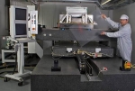
Mask projection imaging of excimer laser pulses for direct ablation has been developed already 2 decades ago. Still today, a very large scale test facility has not been available for research and development purposes until recently. The KrF Excimer lasers emitting at 248 nm with pulses of up to 600 mJ per pulse and repetition rates of up to 400 Hz structure 2 x 1.5 m2 polymer sheets down to 80 micrometer depth of the structures. Strongly differing from the focusing and pixel scanning laser machining systems the mask projection ablation results in unique efficiency. Air bearings, interferometric positioning, short wavelenght and stable lasing are the combined requisites of the laser center @ empa, Thun.
Alternative laser processing with longer pulse duration for laser soldering are presently carried out in our labs. For these applications we apply long pulse, fibre coupled Nd:YAG laser, providing pulses with high power (up to tens of J) and variable length (0.1-20 ms) and intensity controllable fiber lasers. They are ideal for applications including relatively slow dynamic processes such as surface diffusion or even bulk diffusion. Optimizing laser processes can always be carried out by two fundamentally different ways, either adapting the laser parameters, or adapting the materials properties. In our laboratory we focus on tailoring of materials for specific laser applications such as laser debinding, laser sintering, laser soldering, laser welding. If materials are fixed (e.g. for medical applications) we focus on the physical parameters.
Optical materials
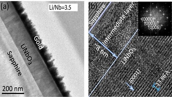
High vacuum chemical vapour deposition technique has been developed during many years in our group for deposition of thin films of oxide materials. Our HVCVD reactor is designed for 4” wafers, healable up to 700°C. Three independent precursor delivery lines are available on the reactor. Precursor behaviour in high vacuum may significantly differ from the observed in standard CVD conditions. Our expertise and research interest include the important part of precursor testing and selection.
Both crystalline, functional (e.g. electro-optic) materials, doping for active laser properties and amorphous films for passive waveguiding functionality have been deposited our the past years. List of materials, which we have been or are working with, includes, but is not limited to LiNbO3, BaTiO3, TiO2, Al2O3, Nb2O3, HfO2, …
Characterization of the thin films’ structural and functional properties is also an important task in the investigations and provides feedback for the fabrication process.
Currently, we are working on the integration of the crystalline materials such as LiNbO3 and BaTiO3 on technological substrates to enable up scaling. Processing methods of thin films on the wafer scale, such as structuring, selective deposition with irradiation by laser or electron beam, lift-off techniques, are critical aspects of integration and device fabrication and also receive high attention in our research.
For more detailled information:


