Material Mechanics
Continuum crystal plasticity simulations
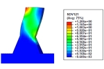
The central aspect in continuum crystal plasticity formulations is the increase in the critical resolved shear stress, needed to activate a slip system, with the interaction between primary and forest dislocations. We perform crystal plasticity finite element simulations of sharp and spherical indentations and micropillar compression on FCC and BCC single-crystal metals. These simulations allow us to anticipate the different active slip systems and extract mechanical properties (using methodologies previously developed also through finite element simulations), taking into account the crystallographic orientation, and provide a theoretical framework to experiments.
Mechanical behavior of a high pressure sensor

Through finite element simulations it is possible to study complex systems under mechanical solicitation. We can define different parts and the interaction between them, apply forces, pressures, temperatures, etc., study the developed stresses and optimize the system on the basis of the obtained results. In the case of a high pressure sensor, we have a glass beam attached on a steel membrane by a binding material. The glass beam is deflected by the application of a pressure on the opposite side of the steel membrane. This system can be modelled through finite elements by assigning mechanical and thermal properties and defining the interaction between parts. This type of analysis allows optimization of the steel membrane and glass thicknesses.
High Temperature Deformation of Ultra-fine-grained (UFG) and Nanocrystalline (nc) Metals
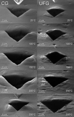
UFG metals offer significant advantages in strength and ductility over metals with conventional grain sizes. The typical method for producing UFG metals is by severe plastic deformation (SPD) using either accumulative roll bonding (ARB) or equal channel angular pressing (ECAP) techniques. The onset of superplastic deformation was observed at lower temperatures for UFG aluminum than for conventional grained material. This was observed to be linked to the activation of grain boundary and lattice diffusion. Strain rate jump tests were effectively demonstrated to measure strain rate sensitivity as a function of temperature below the onset of superplasticity.
For more detailled information:High Temperature Deformation of Bulk Metallic Glasses (BMGs)

The elevated temperature mechanical response of a Zr-based bulk metallic glass (BMG) was examined using in situ indentation and micro-compression in the SEM. This allowed direct observation of shear band formation and propagation as a function of strain rate and temperature as well as measurement of uniaxial stress-strain relationships. The flow stress has been found to remain constant with temperature at ~2 GPa below the glass transition temperature, Tg. The magnitude of the stress drops/serrations in the indentation load-displacement curves, and compression stress-strain curves increases with temperature. Above Tg, plastic flow was observed to be homogeneous without any shear band formation, and the flow stress was observed to decrease significantly. (Materials Science and Engineering, 2011, Scripta Materialia, 2012)
High Temperature Crystal Plasticity of Micro-scale Samples
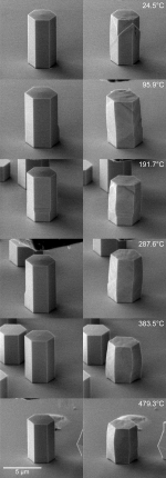
Elevated temperature, in situ micro-compression is a straightforward method for measuring single crystal plasticity parameters. Using micro-scale specimens, this method allows crystal plasticity parameters and deformation mechanisms to be rapidly measured even on brittle materials. By combining this approach with focused ion beam (FIB) machining, the mechanical behavior of site specific micron-sized specimens can be determined as a function of both temperature and strain rate. Slip systems are directly observed via surface steps in situ during deformation in the SEM. By using micro-pillar strain rate jump tests, the strain rate sensitivity and activation volume of materials can be measured even when there are a limited number of specimens available. By combining this technique with electron backscatter diffraction (EBSD), the stress-strain behaviour can also be characterised in relation to crystal orientation.
Mechanical properties of high temperature materials
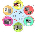
Advanced energy power systems like Generation IV fission reactors, thermonuclear fusion reactors, solar thermal/solar chemical reactors, gas turbines and coal gasification systems require materials that can operate at high temperatures in extreme environments: irradiation, corrosion, unidirectional and cyclic loads. On the path to development of new and adequate high temperature materials, understanding of damage formation and evolution and damage effects is indispensable. Damage of materials in components takes place on different time and length scales. A multiscale approach is needed to develop a unified model of the material behaviour based on dedicated tools to test and analyse materials on different scales. The project part at EMPA concentrates on the determination of irradiation induced changes in stress-strain response of metallic high temperature materials. As the penetration depth of ions produced by conventional accelerators is only a few microns, methods for determination of mechanical properties with sub-sized samples will be explored. On the one hand focused ion beam (FIB) prepared micropillars will be mechanically loaded with a microindenter head in a scanning electron microscope (SEM), allowing for the determination of stress-strain curves. On the other hand stress strain curves will be calculated from nanoindentation experiments via numerical methods. Transmission electron microscopy (TEM) investigations of deformed surface parts will give a correlation between the mechanical properties and the irradiation induced defects. Residual life assessments for service exposed materials will be established via comparison of the results with macroscopic mechanical tests.
Cleavage of III-V laser bars
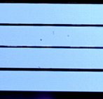
We investigate fundamental phenomena occurring during the scribing and subsequent fracturing process usually performed when preparing surfaces of brittle semiconductors. We showed recently how phase transformation can occur in Si under a diamond tip, how single dislocations can be induced in InP wafers and how higher scratching load of GaAs wafer leads to the apparition of a crack network below the surface. A nano-scratching device, inside a scanning electron microscope (SEM), has been used to observe how spalling (crack and detachment of chips) and/or ductile formation of chips may happen at the semiconductor surface. Cleavage experiments revealed, that breaking load of thin GaAs (100) wafers is directly related to the presence of initial sharp cracks induced by scratching.
Multi-wire sawing of polycrystalline solar cells
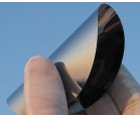
Today, more than 90% of solar cells are produced using multicrystalline silicon (mc-Si) or single crystalline silicon (c-Si). Despite the large research effort world-wide put into alternate technologies (e.g. amorphous silicon (a-Si), organic cells etc.), it will probably require one or two decades before new technologies can reach the volume market and/or efficiency of mc-Si/c-Si (typically between 12-16% at the module level). Silicon ingot material and ingot slicing accounts today to about 1/3 of the total manufacturing costs of solar modules. The loss of raw material (kerf loss) during wafer slicing is approximately 30%. The current average wafer thickness in production is 280-350um. Silicon feedstock prices are increasing dramatically, due to the increased demand and limited supply. The key for break-through lowering of raw material cost, hence a major part of solar cell costs, is the reduction of kerf loss and the ability for slicing thinner wafers. Research at EMPA concentrates on the sub-surface defects (cracks, phase transformations, dislocations) that are introduced during slicing the surface of the wafer and on the correlation of the nature of this zone with control parameters like load and slicing speed. Model experiments are performed for controlled initiation and propagation of microcracks by nanoscratching and nanoindentation to simulate the generation of defects / cracks due to abrasive particle/surface interactions. The commercial goal is to develop a process technology that allows mass production of thin crystalline silicon solar cells, including the cutting of ultra-thin silicon wafers (<150um) via multi-wire sawing.
Deformation behavior of liquid-filled microcapsules

Microcapsules, i.e. hollow spheres with diameters of less than one micron up to several millimetres, have a large variety of applications. They are used in different fields like food industry, pharmacy, cosmetics and cleaning. For many applications the most important properties are wall permeability, adhesion and mechanical properties. This study concentrates on the latter. The deformation behaviour of liquid filled polymer microcapsules is investigated by the analysis of load versus strain curves from micro-compression tests performed with a MTS Nanoindenter XP. Properties like critical load and strain, the stiffness of the capsules and the reversibility of the deformation were determined.
Mechanical properties of bulk metallic glass

The formation of shear-bands in a Zr-based bulk metallic glass (Vitreloy-105) was investigated via in situ scanning electron microscopy (SEM) micro-indentation experiments. The formation of new shear-bands was correlated with displacement bursts visible in the load-displacement data. Surface steps around residual indents are often the result of multiple shear-band reactivations at the same locations. Partial crystallization does not stabilize the deformation process, but leads to further strain localization. Higher loading rates lead to smooth load-displacement curves and, in the case of partially crystallized specimens, continuous shear-band activity was detected.


-
Share
