Micro- and Nanopatterning of Medical Implant surfaces
Local electron beam induced reduction and crystallization of amorphous titania films on conductive substrates
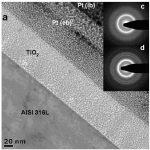
Local electron beam induced reduction and crystallization of amorphous titania films on conductive substrates: We recently succeeded in electrodeposition of uniform films of TiO2, Nb2O5 and ZrO2 valve metal oxides. Local electron beam irradiation can induce reduction and crystallization of electrolytic amorphous TiO2 films deposited on e.g. stainless steel. In-situ substrate temperature measurements and beam heating calculations demonstrate the formation of anatase (Raman) below 270°C, clearly beneath the crystallization temperature of non-irradiated films (440°C). Atomic force microscopy revealed well defined cavities with Gaussian shape. The enhanced e-beam sensitivity of amorphous TiO2 allows for high-resolution patterning of macroscopic films, inducing local changes in oxidation state, phase, topography or even electrical properties.
Electrochemical structuring/modification of titanium-like sur-faces for biomedical applications
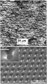
Anodic oxidation of titanium in acid containing electrolytes is a well established technique to increase the thickness of its oxide layer. It is of great value in biomedical applications for improving biocompatibility and corrosion resistance as well as for color coding purpose. Additionally to the chemical composition of an implant surface, also its topography is known to greatly influence the biological response. Besides aiming at a better understanding of film growth, crystallization, incorporation of impurities etc. we study the properties of anodic oxide films in view of its application as natural mask material for subsequent micropatterning via electron and ion beams, as well as via YAG laser irradiation.
For particular interest in applications where chemical inertness, biocompatibility and enhanced osteointegration is desired, we have developed a spark anodization process for Ti and Ti-alloys, resulting in a novel oxide morphology very different from the well-known micro/nano porous oxides on Ti-like materials. These crystalline oxides feature increased open porosity and chemical purity with respect to harmful substrate elements (V, Al, etc).
Advanced chemical and topographical surface patterning of metals is achieved via a combination of maskless (3D) UV lithography and through-mask electrochemical micromachining. This novel approach allows for creation of precise and almost ideal topographies in the micro- to macro range for use in biological cell studies, microfluidics and stamping applications.
Bioactive coatings for implants by electrophoretic deposition
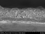
In the field of orthopaedic implants, hydroxyapatite (HA) plasma-spray coatings have been traditionally used in order to enhance implants fixation. However, due to high temperatures, the plasma spray process does not allow for a rigorous control of the final chemical and structural coating properties. Also, it is not straight-forward to deposit a uniform film on complex or even hidden surfaces. Electrophoretic deposition (EPD) is an alternative coating technique with the following advantages: Control of the stoichiometry, uniformity on any shape, flexibility in the choice of materials, simplicity and low cost. We are about to develop graded coatings by EPD, consisting of a biocompatible matrix with well-defined interconnected porosity and bioactive elements with different rates of bioresorbability.
Electrodeposition of energy related materials: from conformal deposition to nanostructures

We study the electrodeposition of n-type ZnO (Band gap ~ 3.3 eV) nanostructures (nano/wires/tubes, urchin-like) with controlled dimensions and morphologies on transparent conductive substrates. The nanostructures were then used as building blocks for nanostructured solar cells. After the deposition of ZnO, we cover these nanostructures by an ultra-thin layer of a light absorber (CdSe) with narrow band-gap (Band gap ~1.7 eV) also by using the electrochemical deposition. To complete the fabrication of the nanostructured solar cell, we fill the space between the core/shell of ZnO/CdSe by a transparent p-type semiconductor (CuSCN) with a wide band-gap (Band gap ~ 3.4 eV) by using electrodeposition or by liquid infiltration followed by precipitation.
Surface patterning through Self-assembly methods
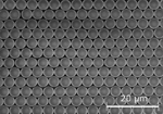
We produce patterns using self-assembly methods (spin-coating or dip-coating) with polystyrene or SiO2 nanospheres for producing mono- or multi-layers onto different kind of surfaces (e.g. Si, TCO, ITO, etc), com-bined with a subsequent electrochemical etching or deposition. We explore then, the possibility of producing highly organized monocrystalline nanodots, nanowires and nanorings onto flat or non-flat surface for diverse applications.
Electrodeposition of TiO2
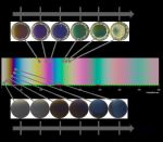
TiO2 is a highly versatile and industrially attractive wide bandgap semiconductor. The oxide can be deposited in near-room temperature baths via electrochemically induced precipitation. However, it is challenging to deposit crystalline TiO2; typically it is amorphous and there are only a few examples of crystalline as-deposited films using additives. We are investigating different additive-containing and additive-free baths to induce crystallinity in our deposits. Toxicity is an important issue for biomedical applications, and the minimi-sation of contaminants from additives is desirable. Interference effects determine the colour of the thin films, and thus the colour of the deposits can also be tuned by varying their thickness.
Electrodeposition of silicon thin films
The electrodeposition of amorphous silicon thin films in organic solvents on transparent conductive substrates is currently investigated. While playing on the bath chemical composition (solvent, precursor concentration, supporting electrolyte) and on the deposition conditions (potential, time), different film morphologies have been obtained. Our main goals are to meet the challenge of stabilizing these Si films against oxidation when exposed to air and to decrease the impurity content. Promising results have been obtained after annealing the films in inert atmosphere as shown by Raman spectroscopy in the illustrating figure.
Physico-Chemical interactions between selected cultural metallic artefacts and indoor environment
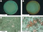
Metallic objects are decoratively colored by patination in all great metalworking traditions over many hundreds of years. A patina is a corrosion layer of various chemical compounds formed on the surface of metals during chemical reactions or exposure to weathering. One example of a patina is a green surface texture cre-ated by slow chemical alteration of copper. Environmental factors in museums can affect metallic (art) objects. For example, zinc and lead objects will be corroded by reactions with formic acid which is emitted by wooden objects and paints. Black spots from copper sulfide are formed on copper objects by reactions with ammonia which is emitted from rubber objects and is also present in ambient air.
We investigate the reactions between pollutants and artificial patinas on copper (Picture). We investigate changes in chemistry and mechanical stability by in-situ spectroscopic and microscopic analysis to find out the mechanisms of interaction.


-
Share

