Microstructural analyses
EBSD

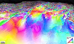
Electron Backscatter diffraction (EBSD) is a SEM based technique that provides crystallographic information from a small volume of material. When the SEM primary beam strikes a crystal, some of the electron will be elastically scattered by the crystal planes and will form arrays of Kossel cones whenever the Bragg condition is satisfied. These Kossel cones can be collected in the SEM chamber by a phosphor screen, where they form a pattern composed of bright bands. Each of these bands corresponds to a lattice plane and the electron backscattered pattern contains therefore information about the lattice structure and orientation. This pattern is recorded by a CCD camera and can be automatically indexed. By scanning the beam on the surface of the sample, a crystal orientation map can be acquired. Information about the crystal structure, the texture, the grain size or the grain boundary type of the materials can be then obtained. In EBSD, the surface of the sample is tilted at 70° from the primary been in order to alloy a maximum of backscattered electron to reach to the phosphor screen. This set-up alloys a spatial resolution between 25 and 100nm depending on the measured material (average atomic number and density) and the electron beam energy (bias voltage and beam current).
We use EBSD to characterize in detail the microstructure of different type of materials, thin film, coatings or nanostructures (nanowires, nanodots and micro-pillars). EBSD can be combined with EDS for more accurate phase recognition. We also use EBSD during in-situ mechanical deformation inside the SEM to follow in detail the progressive deformation which occurs in the material during the loading. Plastic deformation can be assessed by mapping the misorientation gradient in the deformed grains.
TKD

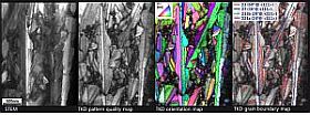
The volume of interaction of the backscattered electrons can be drastically reduced by using EBSD in transmission inside the SEM. This consists of placing a thin lamella (between 100 and 200nm) of the sample at 10 to 40° to the primary beam, in the opposite direction of the usual 70° and at smaller working distance (3 mm). This technique is called Transmission Kikutchi Diffraction (TKD) or transmission EBSD (T-EBSD). A lateral resolution up to 5nm can be achieved, which makes a method of choice for microstructure characterization at the nanoscale. We use this technique to characterize nanocrystalline electrodeposited materials or PVD coatings. The preferred crystallographic growth direction, the grain dimensions or nanotwins size and orientation can be determined, for instance. The microstructure influences a lot the mechanical properties of materials. We use therefore TKD to characterize UV-LIGA micro-mechanical parts and modify the electrodeposition parameters in order to obtain an optimized microstructure, enhancing the mechanical properties of the material.
EBSD Cross-Correlation Technique (HR-EBSD)

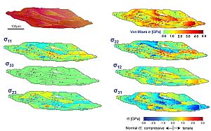
Elastic strain in material can be assessed by measuring changes in interplanar angles in the electron backscattered pattern. This is done by using a cross-correlation technique where one pattern in the measured sequence is used as a reference and small shifts and rotations are measured for a number of regions of interest (ROI) dispersed across the other EBSD patterns. The shifts (x and y components) at the centre of each ROI are related to the components of the displacement gradient tensor, which can be solved into a strain tensor (symmetric part) and a rotation tensor (the antisymmetric part). Knowing the crystal directions from the indexed patterns and the elastic constant for the different crystallographic directions, a full stress tensor can be then determined. Sensitivities of a few hundredths of a pixel can be obtained, bringing a resolution in the order of 10-4 in strain if the pattern quality is high and recorded at full resolution (no binning). We use this technique to measure residual stresses in materials, around grain boundaries, inclusions, indents or in epitaxial layers, for instance. Accurate misorientation measurements can be done, allowing estimation of the geometry necessary dislocation in deformed materials using Nye’s dislocation tensor. We apply also the cross-correlation technique during SEM insitu micorpillar compression to map the strain and the stress distribution in the pillar during the deformation. A precise measurement of the rotation tensor allows also a control the bending of the pillar during the compression.
X-Ray diffraction
We use X-ray diffraction to determine the phase composition of thin films, coatings or bulk materials. Rietveld refinement is used to determine lattice parameters, for phase quantification and for crystallite size determination. Residual stresses are measured using the sin2ø method. Our set-up allows both parallel beam and Bragg-Brentano configurations. We are equipped with a line detector for fast acquisition and an Eulerian cradle for good sample alignment and texture measurements. The line detector can be rotated horizontally for reflectometry measurements, which is used for determining the thickness and density of thin films and multilayer coatings. We are also equipped with an Anton-Paar DHS 1100 heating chamber for in-situ acquisition at high temperature under controlled atmosphere (up to 1100°C). This chamber is equipped with an X-ray transparent dome which allows grazing incident, texture, or strain measurements at high temperature.
The great advantages of X-ray diffraction techniques are: the simplicity of sample preparation, the rapidity of measurement and the ability to analyse mixed phases. It is also non-destructive, meaning that the sample can be directly re-used after the measurements or several measurements can be made at different steps in the sample fabrication process, for instance.
Raman spectroscopy

Raman spectroscopy is a powerful non-destructive optical technique which provides detailed information on the structure of materials, such as chemical composition, cristallinity, lattice strains, defects, and crystal size, by probing their vibrational modes. When combined with an optical microscope, Raman spectroscopy can map the intensity of a definite Raman peak over a portion of the surface of a sample with micrometer lateral precision. For instance, thin films of polycrystalline silicon are being considered for low-cost production of solar cells, but high residual stresses influence both their mechanical and electrical integrity. We have shown that Raman spectroscopy can map these residual stresses, which are found mainly close to grain boundaries with amplitudes reaching GPa values.
Surface-enhanced Raman spectroscopy (SERS)

Raman spectroscopy is a powerful technique for identification of molecules by probing their vibrational modes, but the efficiency of the Raman scattering process is very low, with approximately one emitted photon for 1012 incident photons, thus reducing its applicability to highly concentrated solutions only. However, Raman signals can be tremendously enhanced when molecules are adsorbed on specific metallic nanoparticles. This surface-enhanced Raman spectroscopy (SERS) effect, which can increase the signal by many orders of magnitude, allows us to detect Raman spectra of very low concentrations of molecules. This high sensitivity associated with the spectroscopic wealth of information that can be recorded by SERS presents a huge potential for chemical/biomolecular trace analysis. However, SERS can be envisaged as an analytical tool only if substrates with reproducible enhancement can be produced. Recently, we have tailored new substrates with well-defined nanostructures in accordance with a detailed comprehension of the SERS mechanism. For example, we have fabricated large ordered areas of silver nanoparticles on a Si(111) surface using electroless metal deposition and the nanospheres lithography method. The possibility to control the size, the interdistance and the crystallinity of these nanoparticles allowed us to systematically investigate their influence on SERS, demonstrating the existence of an ideal size because too large particles allow the excitation of nonradiative multipoles whereas too small particles lose their electrical conductance and cannot enhance the field.
Tip-enhanced Raman spectroscopy (TERS)

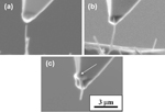
Surface-enhanced Raman spectroscopy (SERS) is based on the increase of the electromagnetic field of light by nanometer-sized metal particles, resulting in a large enhancement of the Raman signal. By replacing the metal particles by the metallic nanotip of an atomic force microscope (AFM), the enhancement can be localized at will. The resulting tip-enhanced Raman spectroscopy (TERS) is capable of measuring Raman spectra with nanoscale resolution, effectively overcoming the diffraction limit. A successful TERS experiment depends heavily on the ability to fabricate tips of a definite metal with the appropriate shape and size, which is still a challenging process. For instance, we have shown that hemispherical gold droplets on top of silicon nanowires grown by the vapor-liquid-solid mechanism produce a significant enhancement of Raman scattered signals. In more recent results, we have shown that silver nanowires attached to AFM cantilevers produce a strong, localized enhancement of the Raman spectroscopy intensity. The nanowires are synthesized by electrochemical deposition inside the pores of an alumina membrane. By subsequently dissolving the alumina membrane, freestanding nanowires are obtained, with an approximate diameter of 200 nm. In the next step, the silver nanowires are attached onto AFM tips by using the electron beam of a scanning electron microscope (SEM) to perform localized electron impact-induced dissociation and deposition. Applications of this novel nanowire-based TERS technique are widespread in the field of solid state research, e.g. in silicon technology where the material composition, doping, crystal orientation and lattice strain can be probed by Raman spectroscopy at the nanoscale.


-
Share
