Nanomechanics
The Nanomechanics Research Group investigates mechanical properties of materials at the nano to macro-scale using experimental, analytical, and computational techniques. Our research interest focuses on understanding the complex behaviour of highly-constrained materials (physical size effect) under mechanical loading for efficient use and high reliability. Emphasis is placed on material properties that substantially deviate from bulk behaviour and thus cannot be extrapolated from handbook values:
- mechanical properties of metal nanowires
- constrained dislocation motion and fracture in micron-sized pillars,
- influence of elastic mismatch in multilayer thin films on dislocation motion
- influence of elastic strain on electronic properties of silicon nanowires.
Failure mechanism in optical multilayer coatings
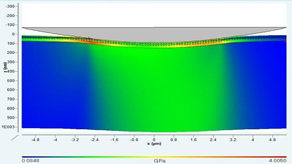
Optimization of the mechanical resistance of ultra-thin multilayer coatings on glass is a complex task. A versatile set of physical constants and properties determines when such a system will fail under mechanical pressure. FilmDoctor software, provided by SIO (Saxonian Institute of Surface Mechanics, Germany), is used to calculate stress-strain fields generated inside each layer and in the glass substrate. Using this software in conjunction with nanoscratch experiments is one of the key that leads to understanding of the failure mechanisms and optimization of such coatings.
Mechanical properties of nanowire arrays
In small-scale mechanical testing, there is a need for specimen with tunable geometry and microstructure. We investigate the mechanical properties of such samples fabricated by electrochemical deposition. Ordered arrays of metallic nanowires with diameters between 30 nm and 1 um and various aspect ratios are tested in compression. In-situ SEM experiments offer a direct observation of the failure mode and give the transition from a buckling collapse to uniaxial compression of the wires, which enables systematic studies on scaling effects.
In situ, High Temperature Indentation and Micro-Compression in the SEM
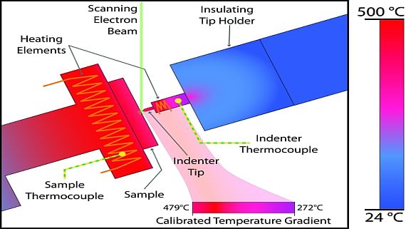
We have developed a modified Alemnis system which is capable of indentation and micro-compression in situ in the SEM at temperatures up to 500°C with drift levels as low as 1 nm/min. The system features water-cooling and independent heating of the sample and the indenter. The system utilizes thermally calibrated indenter tips which act as surface temperature probes, so that not only is indentation performed with low levels of thermal drift but it is also performed with precisely known surface temperatures (Phil. Mag. 2012). This allows thermally-activated deformation mechanisms to be observed and measured simultaneously in the SEM. The high vacuum of the SEM also acts to prevent oxidation of both diamond indenters and metallic samples at high temperatures.
Mechanical and electronic properties of silicon nanowires
We investigate the fracture strength of silicon nanowires grown on silicon substrate by the vapor-liquid-solid process. The nanowires, with diameters between 100 and 200 nm and a typical length of 2 micrometers, are subjected to bending tests using an atomic force microscope setup inside a scanning electron microscope. The average strength calculated from the maximum nanowire deflection before fracture was around 12 GPa, which is 6% of the Young's modulus of silicon along the nanowire direction. This value is close to the theoretical fracture strength, which indicates that surface or volume defects, if present, play only a minor role in fracture initiation.
Mechanical properties of metallic nanowires
Nanowires have attracted considerable interest as nanoscale interconnects and as the active components of both electronic and electromechanical devices. We investigate fundamental mechanical size effects in monocrystalline and nanocrystalline Tungsten, Rhenium and Nickel nanowires and explore applications for acoustical sensors. Combination of experimental tests and theoretical modeling allows determining intrinsic material parameters of nanowires.
Size effects in semiconductor micropillars
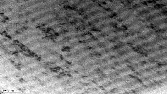
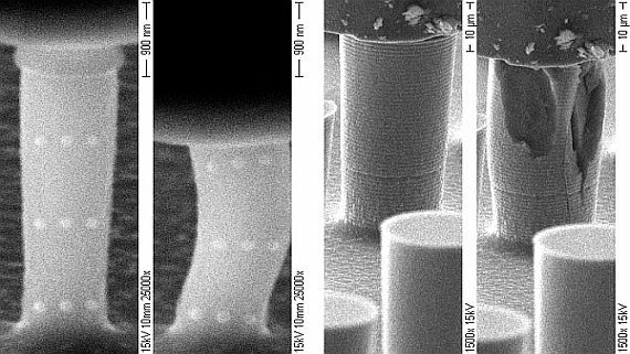
We investigate experimentally the compressive strength of semiconductors such as silicon (Si), gallium arsenide (GaAs) and Indium Phosphide (InP) by taking the traditional uniaxial compression test to the micrometer scale. Contrary to silicon, GaAs micropillars were found to exhibit ductile plasticity at room temperature comparable to that of metal single crystal micropillars. Transmission electron microscopy revealed that the crystals deformed mainly via twinning. This observation is explained based on the high sample surface to volume ratio, which allows for nucleation and absorption of partial dislocations at the surface.
Mechanical properties of multilayers and thin films
We explore scale effects in ultrathin superlattice and multilayer thin films that allow to design superhard wear resistant thin films. One approach is based on the supermodulus effect that describes the drastic enhancement of the hardness of a nanocomposite material composed of two phases having a large difference in their elastic shear modulus, a large internal stress in one of the two phases and structures between 2-3 nm in dimension. Another approach is based on an increased fracture toughness due to a multilayer structure.
Calculation of stress-strain curves from nanoindentation data
The possibility to accurately determine complete stress-strain curves also on the microscopic scale is therefore of vital interest. One promising path is the use of nanoindentation (or instrumented indentation) load-displacement data in combination with numerical simulations. We developed a method for the calculation of true stress – strain curves based on pyramidal (conical) indentation curves.
Instrumentation for Nanomechanics Research
We develop in-situ SEM nanomechanical testing devices (nanoindenter, AFM, microcleaver, microtensile, CNT nanomanipulator etc.) that allow to observe deformation and fracture mechanisms with nanoscale resolution. For instance, looking at the surface of micropillars during deformation allows to identify a sequence of buckling, dislocation, microtwin or shear band nucleation, which enables to setup a microstructure model to describe the physical size effect.
Deformation process of semiconductors
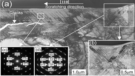
In the last two decades, semiconductors have been widely used in many fields such as MEMS, NEMS and microelectronic industries as well as solar cells and laser industries. We study the mechanical deformation responses of semiconductors such as Si, GaAs and InP to contact-induced damage. The main methods are nanoindentation and nanoscratching. Nanoindentation has become the most widespread method to probe via nano-contact testing the mechanical material properties, to characterize phase transformations or thin film delamination. Nanoscratching is used to scrutinize tribological contacts to produce microstructures by electrochemical trench etching or to create a defect to analyze the subsequent cleavage and fracture of brittle materials.
In-situ Raman micropillar compression
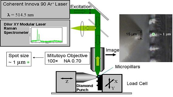
The micro- and nanoscale plastic deformation and fracture behaviour of semiconductor components determines the performance of many microelectronic and microelectromechanical systems. The combination of microcompression and micro-Raman spectroscopy is shown to be capable of detecting crack formation prior to failure, allowing: 1) estimation of in-plane stress in the vicinity of the crack tip, as shown by Wasmer et al. [J. Mater. Res. 23, 3040 (2008)] and 2) distinguishing between ductile and brittle behaviour. Single crystal silicon and gallium arsenide micropillars were fabricated by a focused ion beam (FIB) technique. The mechanical and photonic response of the micropillars were investigated by room temperature in-situ Raman uniaxial compression tests performed with a diamond flat punch using a custom made microindenter instrument (see Figure of the set-up).
