Nanostructuring via electrodeposition
We are interested in materials and structures whose properties can be tuned or optimized by variations in size, geometry, crystallinity, composition or surface. This “make and measure” strategy is applied primarily to problems related to mechanical devices, biomedical materials, culture heritage surfaces, renewable energies and magnetism.
Electrodeposition of metallic micro and nanostructures
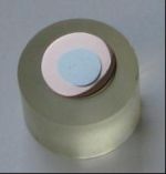
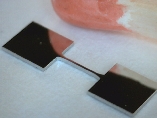
Electrodeposition of metallic nanostructures
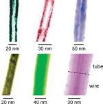

Free-template electrodeposition is used for the synthesis of metallic nano/microstructures on solid substrates in order to facilitate their practical applications as nanobuilding blocks in nanodevices. For tailoring the nanostructures and the growth mechanism, organic molecules can be added to the electrochemical bath. The use of these metallic nano/microstructures in many applications (SERS, gas sensing, wettability, etc) is studied.
Mechanical Properties of electrodeposited structures

Mechanical properties of electrodeposited microstructures and nanostructures are investigated though micro tensile, microcompression and nanoindentation tests. Microdevices, shapes and intrinsic structures are tai-lored during the electrodeposition process. Investigation of mechanical properties of electrodeposited nan-owire is fundamental for the complete correlation between synthesis parameters/nanostructure and physical properties (see above). Combination of experimental tests and theoretical modeling allows determining in-trinsic material parameters of nanowires.
Electrodeposition of metallic microstructures
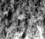
UV-LIGA process for patterning of thick photoresist masks, the development of new alloys for microdevices by means of electrodeposition, having specific and well-controllable properties is the aim of the project. Development of galvanic processes for new and enhanced alloys interesting for microdevices such as NiFe, NiCo and NiFeCr is investigated. We developed a novel plating propeller cell inducing a thin, uniform and non-periodic boundary layer across the entire wafer surface. The temporal uniformity of the diffusion layer thickness is advantageous in the deposition of anomalous alloy pairs because of the compositional dependence on current density.
Combined electrochemical and mechanical nanopatterning of semiconductor surfaces
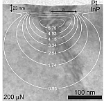
We investigate selective dissolution of n-InP(1 0 0) triggered by surface defects. Nanometer size grooves were produced by sensitizing an InP surface with a mechanical contact patterning technique, i.e. nanoscratching at low loading forces at the threshold between elastic and plastic contacts. Subsequently, site-selective electrochemical dissolution was triggered in acidic electrolytes. Electrochemical characterization shows that there is an onset voltage for selective dissolution at the scratch-induced defects and that it is possible to define a processing potential window where dissolution occurs only inside the nanoscratches. Scanning electron microscopy (SEM) micrographs reveal that for optimized forces, highly confined dissolution in well-defined channels of 125 nm width can be obtained. Transmission electron microscopy (TEM) cross sectional analysis of the scratches before and after electrochemical experiments shows that the dislocations generated are confined in a well-defined volume below the surface, and that exactly this dislocated volume is dissoluted. Based on contact mechanics, the lateral resolution and the morphology of the dissolved groove can be explained by the dissolution time and the tip radius and the morphology by the applied load.
Prediction and Optimization of Electrodeposition Parameters and/or Mechanical Properties of Deposits using FEM tools
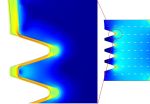
From one side, we develop optimization of the deposition processes by current density modeling during plating process and depending on the bath composition and substrate shape.
Internal stresses of the deposits depending of the synthesis parameters are then tested in order to produce a FEM modeling of the stress distribution depending on shape and synthesis parameters of the deposits.
A theoretical FEM model for electrodeposition is developed. With this model, we predict and optimize the parameters for electrodeposition of nanostructured materials or alloys. This is made, in order to improve the composition of the electrodeposited materials, and therefore, their mechanical properties.
These optimized parameters are compared with experiments, and then used to improve the bath composition and current density applied during the electroplating process, allowing us to obtain the desired mechanical properties, composition and patterning of the deposited material.
-
Share

