Services
Our solution to your problem
The topics of our high quality services are closely related to our research activities. For applied research for industries, SMEs, associations, federal agencies and private customers we maintain a modern and efficient testing infrastructure and analytic equipments. We characterise in particular mechanical properties of materials, provide state of the art surface and microstructure analysis facilities and offer prototyping facilities for surface patterning via UV-, electron- and ion beam patterning methods.
Electron Microscopy
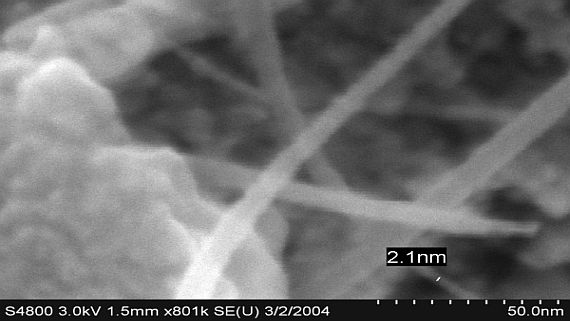
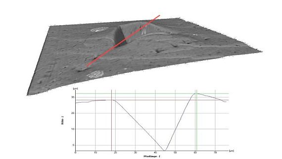
Our electron microscopy lab offers high-quality imaging. Different microscopes for different purpose are available. A Hitachi S-3600 with variable pressure is used for common work and electron beam lithography. For high resolution imaging our Hitachi S-4800 is the best choice. This electron microscope is equipped with analysis tools like EDX, EBSD and STEM. The Zeiss DSM 962 has the function of a micromechanical testing lab. Specialized equipment allows us to perform micromechanical testing (indentation, tensile, compression) inside the scanning electron microscope. A special 3D backscatter detector allows us to get three dimensional images. Calculations like depth profil, volumes and more can be performed.


Mechanical testing on microscopic and macroscopic scales
We offer mechanical testing on the macroscopic scale (tensile and bending tests, hardness measurements, adhesion tests) as well as on the microscopic scale (nanoindentation, nanoscratching, microcompression). A speciality of our lab is micromechanical testing inside the scanning electron microscope (indentation, tensile, compression) that allow a real-time observation of the sample during deformation.

Chemical and microstructure analysis
Nanomechanics
We offer nanoindentation, nanoscratching, micro-tensile, micro-bending tests on a mandate basis.
We provide state of the art electron microscopy facilities including ultra-high resolution SE and BSE imaging, FIB, EBSD, EDX and STEM techniques.
Nanostructuring via electrodeposition
We offer scientific advises on the electroplating bath development for UV-LIGA process and others. We offer advises with galvanic processes and related mechanical and structural properties to be investigated. We also have competence for anodisation processes. In detail:
- Developed electroplating bath for UV-LIGA process
- Galvanic processes and related mechanical and structural properties.
- Anodisation processes (e.g. Al…).
- Optical properties (Transmission and reflectance) of different kind of semiconducting and metallic materials by using Spectrophotometer connected to integrated spheres.
- Photoconversion efficiency measurements (I-V curves) of solar cells using halogen light source.
- UV-lithography facility

