Large Area Perovskite Solarcells
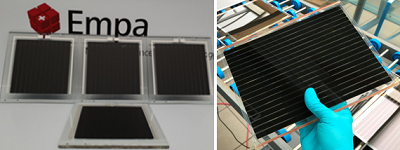
Thin film solar cells based on hybrid organic-inorganic salts with perovskite structure are considered to be the most promising technology for low cost, large-scale photovoltaic energy conversion. This new approach has literally overrun most of the competing efforts focused on high-throughput solution coated devices.
At Empa, we develop printing and coating processes for the up-scaling of Perovskite solar cells manufacturing.

The project PEROPRINT was carried out by EMPA in the facilities of the Coating Competence Center and Solaronix, a Swiss company serving customers worldwide with expertise in photovoltaics, from materials production to solar panels and testing equipment manufacturing (www.solaronix.com). In Peroprint we could demonstrate that Perovskite solar cells can be manufactured by slot die coating. Peroprint was a Cleantec pilot- and demonstration project funded by the Swiss Federal Office of Energy (Projekt-Nr. SI/501237).
The follow-up project UPero aims to scale-up an efficient production process while reducing the thermal input and increasing the coating speed. The results shall foster the industrialization of this young thin film technology. The present project UPero shall establish the groundwork for industrial large-area production.
Upero is a Cleantec pilot- and demonstration project funded by the Swiss Federal Office of Energy (Projekt-Nr. SI/501816).
The developments resulted in the foundation of the company Perovskia:
Reference:
Verma, A. et al., Towards industrialization of perovskite solar cells using slot die coating, J. Mat. Chem A, 2020, https://doi.org/10.1039/D0TC00327A
Verma, A. et al., Inkjet printed mesoscopic solar cells with custom design capability. Materials Advances, 2020, 1, 153-160, https://doi.org/10.1039/D0MA00077A
Laser Scribing
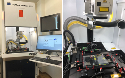
Our lab hosts a laser unit (TruMark 3330 from Trumpf). The UV laser (355nm (ultraviolet) Nd:YVO4) is primarily used to scribe the interconnects of printed or coated large area Perovskite solar cells. The substrate holder is able to handle substrates up to 300x300 mm size.

Scribing laser unit

Examples of laser scribed lines in Oxide layers
-
Share
