Improving the efficiency of semiconductor technology

Less is More – More Energy from the Thinnest Wafers

Oct 10, 2007 | SABINE BORNGRÄBER
The photovoltaic industry is growing at an annual rate of about 35 per cent. However, this upward trend in the development of environmentally friendly solar power is being hindered by the costs of manufacturing solar cells and by the dwindling availability of silicon. If the new technology is to establish itself in competition with conventional methods of energy generation, then the manufacture of solar cells in industrial quantities must be accomplished using smaller quantities of the expensive raw material, silicon, and in addition the performance of the finished product must be yet improved. Empa researchers together with an industrial partner are therefore testing a method of tripling the manufacturing yield. The trick to success in this project, which is financed by the CTI, the Swiss Innovation Promotion Agency, is to cut the solar cells into wafers which are only 100 microns thick instead of 300 microns, as in conventional production.
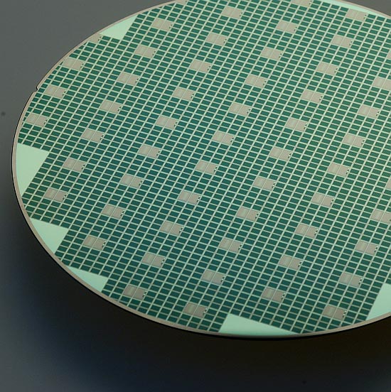
a592-2007-10-10-b0x+stopper+wafer-scheibe.jpg
 

A conventional wafer is 300 microns thick. Optimized techniques will make it possible in future to cut silicon wafers which are only 100 microns thick.


Meeting our energy needs by the use of renewable sources is one possible way out of the global energy and climate crises. Exploiting the energy of the sun’s light is an obvious and attractive method – in exactly one hour and six minutes the sun supplies the earth with the same amount of energy as the world consumed in the whole of 2006! With the help of solar cells, made of semiconductor materials, a small fraction of this energy is captured and converted into electricity. “As soon as people hear the word semiconductor, they immediately think of chips for lasers and computers, or of advanced optical and electronic gadgets”, says Johann Michler, the head of Empa’s Mechanics of Materials and Nanostructures Laboratory in Thun. “It is actually only due to the cleverness and hard work of the material scientists and the mechanical engineers that the manufacture of these devices is possible.” For example slicing a silicon crystal the size of a boulder a meter across into wafers which are only a quarter of a millimeter thick. Or sawing hundreds tiny, perfect chips out of such thin wafers.


More surface area from a block
Despite the many attempts to develop alternatives to silicon-based technology, to date the industry almost exclusively uses “gray gold” – silicon in either its crystalline or amorphous form. When working with the high-value monocrystalline form the challenge is to saw as many wafers from the silicon block as possible, in the shortest time and with the minimum of wastage. The saw which is used for this purpose consists of a very fine wire. This is wrapped around the silicon block several times so that many slices are cut simultaneously. So how does one obtain more surface area from a solid block of material? Simply by making the slices thinner, according to Empa scientists. “In order to optimize this process, we have to understand what happens during the cutting operation”, says Kilian Wasmer, who is responsible for the solar cell project. Wastage during the sawing process can quickly become very expensive, since the silicon costs CHF 250 per kilogram. The material is brittle and during the process fine cracks about 20 microns deep appear on the cut surfaces. With conventional wafers, which are 300 microns thick, these cracks are etched away on both sides. The wastage rate during this process is currently around 30 per cent.

 
Size: 52 KB
Scanning electron microscope image: the Empa researchers are using a very fine diamond pyramid, the nanoindentor, to investigate how cracks occur during the scribing of silicon wafers.
 

Lowering costs by reducing wastage
In order to make the wafers thinner, the researchers must find a way to make these microcracks smaller. Halving the crack depth to about 10 microns would be “a great step forward”, according to Wasmer. Together with a colleague, Adrien Bidiville, he is investigating the processes which cause these cracks to appear for the industrial partners HCT, a manufacturer of these so-called multi-wire saws. Initially, the scientists measure various cutting parameters such as the size of particles on the cutting wire or the cutting speed.

 
Then, based on the data they have collected, they conduct experiments modeling the actual cutting process. With the help of a very fine diamond point – the nanoindentor – they create microcracks in silicon wafers and observe how these are formed and how they propagate in minute detail under an electron microscope. Only when these steps are completed will Wasmer be in a position to develop a concept for optimizing the cutting process. Wismer is sure that “the commercial significance will be quite considerable, since potentially it should be possible to save up to a third of the costs.”
 

Latest know-how for the industrial partner
Michler’s team has just ended a similar CTI project which went so well that it was celebrated as a «Success Story» in the Innovation Promotion Agency’s (CTI) annual report. In this project too the subject was cracks, although this time not in silicon wafers but in microscopic laser components. These are cut out of gallium arsenide wafers, and are so small (their width and height are just 300 micrometers each, and their length is only 2 millimeters) that 40 of them can fit comfortably in a single square on a sheet of graph paper. And at US$ 150 a throw, they are rather expensive, so any wastage here is highly undesirable too. This, however, was exactly what happened to the industry partner, Bookham Switzerland AG, a major manufacturer of laser diodes, whenever the edges were not absolutely smooth during the cleaving of the gallium arsenide wafer. On the scale of the laser element dimensions, even the agglomeration of individual gallium arsenide molecules leads to unevenness which makes perfect cleaving impossible. In addition, during the scribing of the wafer nanocracks developed.


Technology transfer – a win-win situation
Michler and Wasmer used a special nanocleaver to investigate how cracks develop during the wafer cleaving process. As they are currently doing for the solar cell project, they proceeded in three steps. “The solution to the problem”, say Michler, “was to stop scribing. Instead we used the diamond pyramid as a wedge, pressing it into the wafer which we then fractured.” The industrial partner was suitably impressed, and was able to optimize the wafer cleaving process appropriately. As a generous thank-you from Bookham, Michler’s laboratory was allowed to keep the instrumentation which the company had made available for the project – hardware to the tune of half a million Swiss francs. This welcome addition to the laboratory infrastructure will be used in future for the benefit of other nanomechanical projects.

Editor
Dr. Sabine Borngraeber, freelance journalist, Basel

Technical information
Dr. Johann Michler, Mechanics of Materials and Nanostructures, Tel. +41 33 228 46 05,
Dr. Kilian Wasmer, Materials Technology, Tel.+41 33 228 29 71,