Joining technology
With nanoeffects towards new joining processes
Electronic components are becoming smaller, more complex and more powerful – this calls for new solutions for joining them. An Empa team is developing nanostructured joining materials for the next generation of microelectronics and other demanding applications.

Gordon Moore was right. In April 1965, the US engineer and later co-founder of Intel predicted that the number of transistors on a chip would double about every two years. To this day, this development continues with nearly the same speed – also because chip manufacturers worldwide use Moore's Law as the basis for their strategic planning. Thus, the prophecy is self-fulfilling.
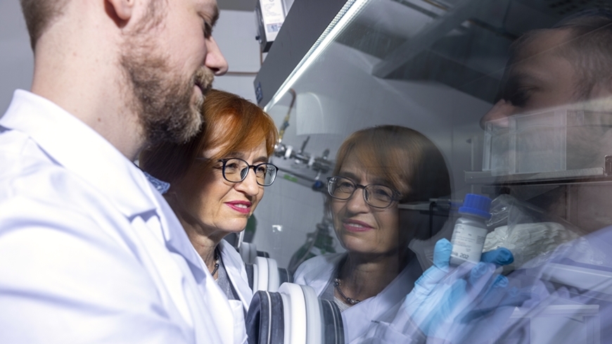
But the doubling of the number of circuits every two to three years sometimes reaches the limits of what is technically feasible. This also holds for the joining technologies, which have to keep up with the increased demands. After all, the ever smaller and more powerful electronic components still have to be integrated into larger systems, and the joints connecting the components to heat sinks or circuit boards should not fall apart during temperature changes or vibrations, or overheat during operation. A team led by Jolanta Janczak-Rusch and Bastian Rheingans from Empa's Laboratory for Joining Technologies and Corrosion is tackling this problem.
Industry in need
"Our partners and customers, for whom we develop customized solutions, always want more, and preferably everything at the same time," says Janczak-Rusch. A joint for a new high-performance electronic component, for example, should be made at the lowest and gentlest possible temperature – and yet survive the highest possible temperatures when the component is in operation, and efficiently dissipate waste heat from the components. This is the only way to combine miniaturization and increased performance without at the same time increasing the cost of cooling to infinity. Other advancing technologies such as photonics, sensor technology, space travel, batteries and turbine construction are also dependent on innovative joining concepts.
New materials and processes are therefore needed to meet the increasingly complex demands placed on joining. In this situation, joining with nanomaterials, so-called nanojoining, offers great potential. Industry is already using silver nanopastes, i.e. joining materials consisting of silver nanoparticles. The advantage: While the melting point for pure silver is 962 degrees Celsius, silver nanopastes can be applied to produce electrically and thermally highly conductive joints at temperatures as low as 250 degrees Celsius. And even better: Once produced, these joints can even withstand an operating temperature above their production temperature.
Utilizing nanoeffects

There's a lot of materials science know-how behind this innovative solution. "Here we are replacing a classic soldering process with a sintering process," explains Rheingans. This means that the particles in the joining zone are not melted, but grow together into larger particles and grains by diffusion, thereby reducing their surface energy. Diffusion, i.e. the movement of individual atoms, is very rapid at surfaces and interfaces. Since nanoparticles have an extremely large surface area in relation to their volume, sintering is particularly pronounced on the nanoscale and can be exploited even at comparatively low temperatures. In the case of very small nanoparticles or thin nanolayers, the amount of easily moving, "liquid" surface atoms becomes so large that the melting point can drop several hundred degrees below the melting point of the solid material. The researchers call this effect MPD (Melting Point Depression) – and use it to develop innovative and efficient joining processes.
The race continues
"We are working on nanopastes with multiple components to optimize the properties of the joining compound and to open up new areas of application," Rheingans says. "For example, we are investigating combinations of copper and nickel nanopastes." These metals are less expensive than silver and exhibit very interesting electrical and thermal properties – but because they are less noble metals, they oxidize much more easily. That has to be prevented in the joining process. "So we put the nanoparticles in a paste of organic adjuvants that evaporate during the joining process and reduce the oxide on the particle surface. Or we coat the particles with a protective coating," explains the Empa researcher. Using special analytical methods such as X-ray diffraction (XRD) or X-ray photoelectron spectroscopy (XPS), the researchers can verify whether the postulated method of protecting the nanoparticles works as intended.
But innovation is also possible with the well-known silver nanopaste: "In an Empa research project for the development of oxide membranes for microelectronics, we were able to effectively support our colleagues with our know-how: using the nanopaste, we could transfer the ultra-thin membranes onto a carrier substrate without introducing any damage," says Rheingans. This method could also be applied to other 2D materials.
An oven on the nanoscale

For particularly temperature-sensitive components, the researchers have another nanojoining method that they are continuously developing further: so-called reactive joining. In this process, reactive foils replace the soldering oven as a local source of heat. The foils consist of a large number of individual nanolayers, for example of nickel or aluminum. When these nano-multilayers are ignited, the nickel and aluminum react and form a new chemical compound – and release a great deal of heat that drives the process and makes it travel at speeds of up to 50 meters per second over the entire foil. Only layer thicknesses in the nano-range enable such a fast and self-perpetuating reaction. Locally, temperatures of up to 1000 degrees Celsius can be reached, but because of the low thickness of the reactive foil, the total amount of heat remains small and limited to the adjacent solder layers. In this way, sensitive electronic elements can be gently and firmly attached to copper heat sinks.
Nanolayer systems to combat heat buildup
An important focus in recent years has been the development of nanomultilayer systems starting from classic brazing filler metal/alloys such as copper, silver, silver-copper or aluminum-silicon: "Due to the lowering of the melting point and the rapid diffusion on the nanoscale, these bonding materials offer the possibility of carrying out joining processes much faster and at significantly lower temperatures than with conventional brazing techniques" explains Janczak-Rusch.
Nanomultilayers can also be used elsewhere in the joining process: With the recently approved SNF-NCN Lead Agency project "Development of submicro- and nanostructured Cu-Mo composites with tailored properties for thermal management," the Advanced Joining Technologies team is addressing the burning issue of heat dissipation in miniaturized electronic components.
"The interesting properties of copper-molybdenum composites have already been used in the design of an ion source for the JUICE mission of the European Space Agency ESA," says Empa researcher Hans Rudolf Elsener, who specializes in space missions. Together with Polish researchers, the potential of nanostructured Cu-Mo multilayer systems as heat sinks will now be specifically investigated and suitable joining processes for their integration will be developed.
Glossary Joining techniques
Soldering/Brazing: The base materials are joined together by melting an additional material, the solder/brazing filler alloy. The workpieces themselves are not melted or fused during the process. Up to 450 degrees Celsius, this is referred to as soldering, and above 450 degrees as brazing.
Welding: In contrast to brazing, the workpieces are partially melted and are immediately joined after cooling. Filler materials are often introduced into the weld seam to increase the amount of molten metal.
Nanojoining is a new scientific discipline. It includes joining techniques for joining nano-objects, but also novel, high-performance joining processes that utilize nano-effects. Empa is one of the main players in this new discipline, as well as a founding member and headquarters of the international Nano- & Microjoining Association.
Prof. Dr. Jolanta Janczak-Rusch
Joining Technologies and Corrosion
Phone +41 58 765 4529
jolanta.janczak-rusch@empa.ch
Dr. Bastian Rheingans
Joining Technologies and Corrosion
Phone +41 58 765 4371
bastian.rheingans@empa.ch
Dr. Michael Hagmann
Communications
Phone +41 58 765 4592
redaktion@empa.ch
-
Share


