New production process for perovskite cells
Fast and cheap track to new types of solar cells
The semiconductor perovskite is seen as a new hope to bring the production price of solar cells down below that of silicon used so far. Empa is developing new manufacturing processes to make perovskite solar cells not only cheaper but also faster to produce and make them ready for industrial use.

Since the development of the first perovskite solar cell in 2009, its efficiency is now equal to that of a conventional silicon cell. However, it still had some weaknesses in the beginning; for example, due to its structure and the materials used, it is very sensitive to moisture, oxygen, heat, UV light and mechanical stress. This makes the cell less durable. Michael Grätzel and Hongwei Han found a solution to this problem in 2014, when the two EPFL researchers developed a cell with a mesoporous framework of oxides and carbon. But this idea was not yet marketable.
At least until now: Frank Nüesch, Head of Empa's Functional Polymers Department, and his team have been working intensively in recent years on new manufacturing processes for precisely these solar cells in order to produce them not only faster but also cheaper. To this end, the researchers collaborated with Solaronix SA, a company based in western Switzerland, as part of a project of the Swiss Federal Office of Energy (SFOE). Together they produced a functional perovskite cell on a laboratory scale with a surface area of 10x10cm.
Slot-die instead of screen printing
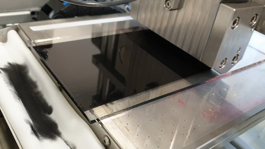
For the production of this novel perovskite cell, the so-called slot-die process is used. Here, the material layer is applied to a substrate of glass and then structured by removing excess material with a laser. "With the new coating process, we can not only coat faster, but also determine the thickness of the layers more flexibly," says Nüesch. In the future, the slot-die process will make it possible to coat meter-long webs relatively easily and quickly. The coating speed is then also the central element in a possible industrialization of perovskite cell production.
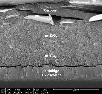
A total of five layers of different materials, including titanium oxide, zirconia and graphite, are required for such a cell. Whereas in the screen printing process used so far, the layers have to be dried and sintered (i.e. compacted) individually - which takes a lot of time and energy - in the slot die process all layers can be applied directly one after the other and sintered together. "With this new process we can 'print' seven times faster than with the previous screen printing method," explains Nüesch. The perovskite solar cell gets its final touch by applying the perovskite absorber by means of inkjet printing in Empa's "Coating Competence Center" - the so-called infiltration. Here the perovskite is no longer applied to the substrate as a solid layer, but seeps through all the porous layers of the solar cell down to the bottom.
A successful cooperation
In developing the new process, the Empa team worked closely with Solaronix experts. They are the source of the "inks" - nanoscale conductors, semiconductors and insulators - for printing the individual, wafer-thin layers of the solar cell. The difficulty for the Empa researchers was to prepare this ink in such a way that it was suitable for the slot-die process. The various settings of the coating unit, such as the speed of the slot-die, the flow rate and the distance between the slot-die and the substrate, also had to be coordinated in order to achieve an optimum result. Now they have succeeded in doing just that.
A further advantage of the perovskite solar cells produced using this new process is a longer service life compared to previous perovskite cells. In a next step, field tests will follow: at the end of 2020, the perovskite solar cells will be mounted on the roof of the NEST building on the Empa campus in Dübendorf, where they will have to prove themselves in everyday use.
-
Share


