Boosting European competitiveness in photovoltaics

Empa joins consortium to develop solar cells

Jul 13, 2012 | MARTINA PETER

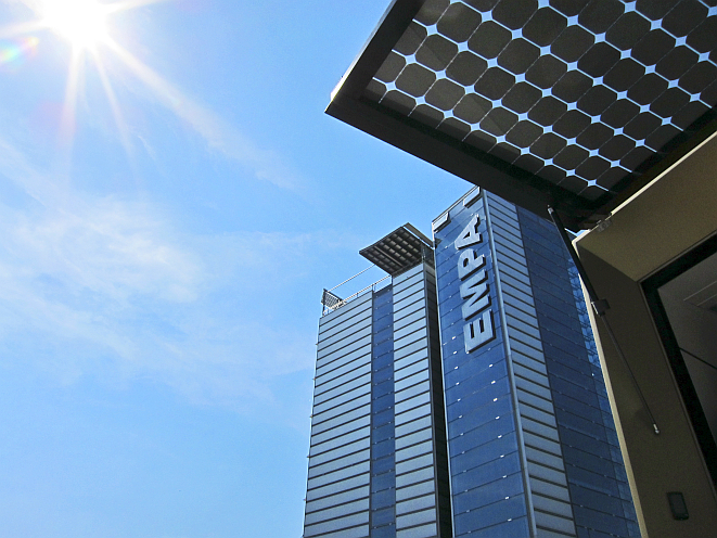
With 13 partners from all over Europe, Empa, the Swiss Federal Laboratories for Materials Science and Technology, has launched an EU-funded project to develop affordable, more efficient solar cells. With an overall budget of 10 million Euro, the SCALENANO project aims at achieving breakthroughs in the cost-efficiency of photovoltaic devices and modules based on advanced thin film technologies.
a592-2012-07-13-scalenano-b1m.jpg
 

Thin film solar cell technologies have a potential to offer a higher material utilization and lower module costs compared to classical wafer-based silicon solar cells because they employ light-absorbing materials that are about 100-times thinner than silicon wafers. Devices based on the substance class of chalcogenides, such as copper indium gallium (di)selenide (also known as CIGS), exhibit the highest efficiencies of all thin film photovoltaic technologies and have already entered the stage of mass production. However, current production methods typically rely on vacuum-based deposition processes that are difficult to control over large surfaces and require expensive equipment. This counteracts the potential reduction of material costs that are inherent to thin film technologies.


To take up this challenge, the EU-funded international project SCALENANO (“Development and scale-up of nanostructure-based materials and processes for low-cost, high-efficiency chalcogenide-based photovoltaics”) – which runs until mid-2015 – will develop alternative, vacuum-free processes based on the electro-deposition of nanostructured precursors. The project also includes the exploration and development of alternative processes with high-throughput and process rates, as well as their extension to the next generation of Cu2ZnSn(S,Se)2-based absorbers (so-called kesterites) that only use cheap and abundant elements. Altogether, this should be a strong boost for European competitiveness in photovoltaic technologies.


Empa’s laboratory for Thin Films and Photovoltaics, led by Ayodhya Tiwari, will contribute to the project by investigating solution- and nanoparticle-based deposition of kesterite absorbers, front electrical contacts of transparent conducting oxides (TCOs) and supplying reference solar cells prepared by vacuum-based techniques. Project leader Yaroslav Romanyuk anticipates that “SCALENANO findings may find applications not only in photovoltaics but also in other fields such as smart windows and batteries.”