Investigating nanopillars

Silicon brittle? Not this kind!

Oct 8, 2009 | MARTINA PETER
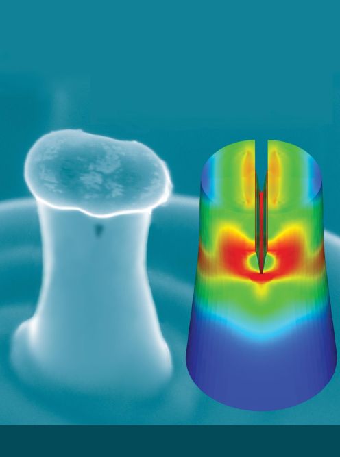
Silicon, the most important semiconductor material of all, is usually considered to be as brittle and breakable as window glass. On the nanometer scale, however, the substance exhibits very different properties, as Empa researchers have shown by creating minute silicon pillars. If the diameters of the columns are made small enough, then under load they do not simply break off, as large pieces of silicon would, but they yield to the pressure and undergo plastic deformation, as a metal would. This discovery opens the way for completely new design techniques from a materials point of view for mechanical microsystems and in the watch industry.
/documents/56164/286256/a592-2009-10-08-MM-Siliziumsaeulen-b1m.jpg/571dbf75-50e8-4a98-959c-54e0d0d7334c?t=1448305883447
 
Empa’s founder himself, Ludwig von Tetmajer, investigated the mechanical loading of columns in his time. In the aftermath of the collapse of a railway bridge in Muenchenstein his laboratory experiments showed that Euler’s bending formula is not always valid for thin rods and needed correction. “We’re basically doing the same thing 127 years later on the nanometer scale, and are learning surprising things – instead of fragile silicon nanocolumns that break when loaded, we are seeing how they undergo plastic deformation like butter,” explains Johann Michler, Head of Empa’s «Mechanics of Materials and Nanostructures» laboratory in Thun.
 

Silicon – the most important material in the semiconductor industry
Silicon is the most commonly used raw material in the semiconductor and photovoltaic industries. It also serves as the basic building material for electronic components (like computer processors) and in many sensors and micromechanical systems, such as the cantilever arm in a scanning force microscope. In addition, more than 90 per cent of conventional solar cells are made of silicon.

But the material has its limits, for silicon is a brittle element – a wafer of silicon (the thin disc of silicon and other additives which forms the substrate for the applications mentioned above) shatters into a thousand shards under the slightest load, just like a sheet of glass. Michler and his colleagues have now shown that this property changes on the nanometer scale. To demonstrate this physicist Fredrik Oestlund treated a silicon plate using an FIB, a Focused Ion Beam instrument which is used for the analysis and preparation of surfaces. Using a beam of gallium ions he removed ring-shaped zones of material from the plate, layer by layer, leaving only tiny pillars of silicon standing. The diameters of the pillars varied between 230 und 940 nanometers.


Size: 78 KB
  A silicon pillar with a diameter of 310 nanometers a) before loading and b) after deformation. The column has yielded to the applied force and undergone plastic deformation.


Load experiments with a nanoindenter
«Our pillar-bending tests are in principle the same as Tetmajer’s experiments, only our pillars are about a hundred thousand times smaller,» says Michler. To apply a force to the columns the scientists used a micro- and nano precision tool called a nanoindenter, where the flattened tip of a pyramid-shaped diamond tool, mounted in a scanning electron microscope, presses down along the longitudinal axis of a silicon column. The force exerted by the tip is continuously measured. «Larger» pillars developed cracks when loaded and broke into small pieces, showing the typically brittle behavior of silicon.

However, when the columns had diameters of less than 400 nanometers, no cracks developed and the structures began to suffer plastic deformation. The reason for this lies in the internal structure of the silicon – its material properties are not determined by the perfect arrangement of the atoms but by the flaws in the arrangement. If the dimensions of the column are smaller than the average distance between defects in the atomic structure of the material then the columns can easily be deformed. Oestlund and Michler, together with their research partners from the Universities of Uppsala and Minnesota, recently published these results in «Advanced Functional Materials», a respected international scientific journal.


Size: 182 KB
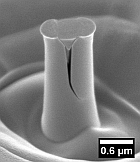
  A silicon pillar with a diameter of  940 nanometers 940 after the compression test. Pillars with a diameter in excess of 400 nanometers develop cracks when loaded.


Silicon with metallic properties
«Our results show that it might be possible to use silicon like a metal in mechanical applications, if the dimensions of the silicon structure are small enough,” Michler speculates. Metallic materials are fault tolerant and are capable of absorbing shock loads by deforming without breaking, for example. The construction of mechanical components using brittle materials is also difficult, since they tend to fail when the strain near a defect becomes excessive. And since the precise location and size of critical defects are practically always unknown, the critical load can almost never be calculated exactly. This calculation is much simpler with a metallic material, which will simply deform under a well-defined load. This new “well-behaved” property of plastic deformation in silicon opens new opportunities for the watch industry and in semiconductor manufacturing in terms of the design of mechanical micro and nanosystems.


Further Information


Editor/Media contact:

 
References

Oestlund, F., Rzepiejewska-Malyska, K., Michler, J. et al.: Brittle-to-Ductile Transition in Uniaxial Compression of Silicon Pillars at Room Temperature, Adv. Funct. Matter. 2009, 19, 2439-2444
DOI: 10.1002/adfm.200900418
The cited paper is available on request from .