Electron Microscopy Center
Empa's Electron Microscopy Center located in Dübendorf offers electron microscopy services to internal and external R&D partners. The center conducts forefront research in the development and application of new electron microscopy techniques in materials science and acts as a consulting unit for electron microscopy in materials science. The staff of the center carries out research tasks on-demand, offers training and provides hands-on support for practical applications.
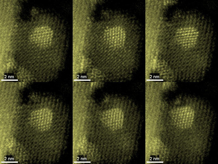
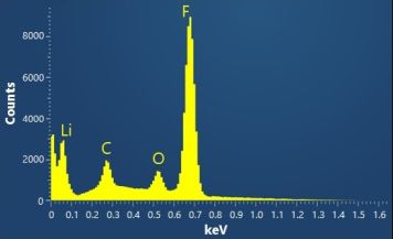
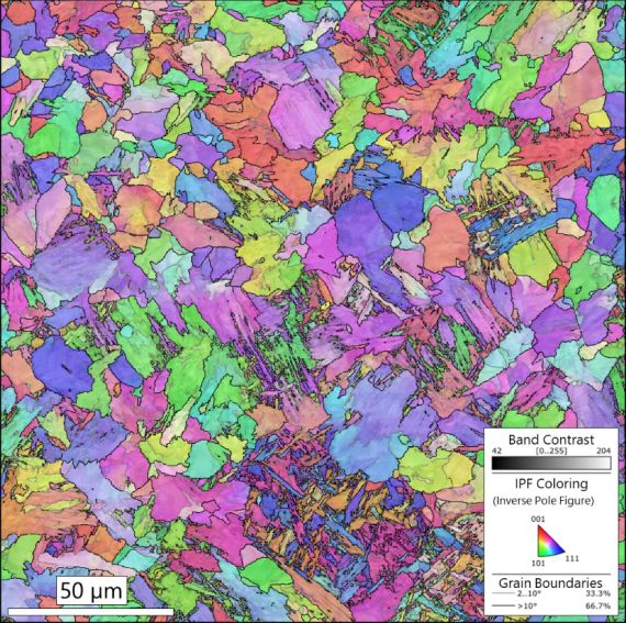
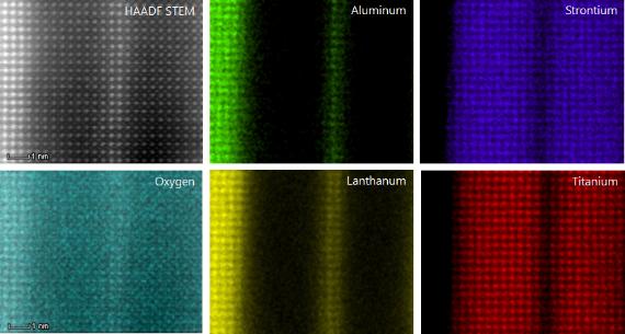
The center operates transmission electron microscopes, scanning electron microscopes and facilities for specimen preparation. Besides convention electron optical imaging (TEM & SEM), the instrumentation can be used for environmental and low-voltage SEM imaging, electron diffraction, atomic-resolution imaging by HRTEM and (aberration-corrected) STEM (Z-contrast imaging), and for analytics, covering high-efficiency EDX spectroscopy (TEM & SEM), electron backscatter diffraction (EBSD), electron energy-loss spectroscopy (EELS) and energy-filtered imaging (EF-TEM). A list of the available instrumentation can be found here.
Our expertise comprises various imaging and in particular atomic-resolution microscopy techniques in the broad-beam and the scanning transmission modes, core-loss and low-loss electron energy-loss spectroscopy as well as electron tomography, in-line and off-axis electron holography for mapping electrostatic and magnetic fields at various length scales as well as differential phase contrast (DPC) STEM, which provides an alternative method to access electrostatic or magnetic information about the specimen. Furthermore, some of our research activities focus on in-situ measurements in (S)TEM using MEMS-based liquid-cell and biasing/heating specimen stages. The experimental work is complemented by image simulations and by first-principles theoretical approaches to calculate electron energy-loss spectra of model structures. For the different simulations, software packages and workstations are available.
More information about our research activities can be found on our research website.
Members of the electron microscopy group work on various research projects involving functional oxides, catalytic metal clusters, as well as tomography and in-situ methods.
Our core expertises are:
- Atomic-resolution imaging in STEM and TEM
- Core- and low-loss EELS
- Elemental mapping by EDS, EELS and EF-TEM
- Electron tomography
- DPC STEM
- In-line and off-axis electron holography
- In situ microscopy: liquid-phase, electrical biasing and heating
- Advanced data analysis methods and simulations

- July 2024: Yifan Zhao successfully defended her master thesis at UZH on 4 July 2024: Design and Microstructural Characterization of Free-standing Ferroelectric Membranes.
Congratulations!
2nd edition (2015): available here


