Micro-chemical analyses
Novel research in nanomechanics and nanostructuring requires specialised instrumentation, not all of which is available commercially. The microanalysis group within the Laboratory for Mechanics of Materials and Nanostructures has
- glow discharge instruments which are used for (quantitative) chemical depth profiling with nanometer depth resolution and part per million level detection limits. We have both GD-OES and GD-TOFMS instruments.
- a Raman microscope, capable of also using the surface-enhanced and tip-enhanced Raman effects (SERS and TERS respectively). This can be used for stress mapping on a sub-micron spatial scale.
- a high spatial resolution Secondary Ion Mass Spectrometer (SIMS), integrated within a dual beam SEM-FIB instrument. This is used for chemical imaging (including depth profiles) on a smaller spatial scale than can be accessed by the glow discharge instruments.
GDOES
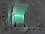
GDOES Elemental Mapping
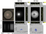
GDOES Simultaneous Determination of Optical Properties and Elemental Composition of Trans-parent Thin Films.
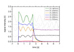
Several novel thin film (TF) solar cell concepts have transparent conductive oxide (TCO) films serving as a front contact. The electrical and optical properties of such films can be tuned by varying their composition. Zinc, as opposed to other typical elements used for conductive oxides, is a relatively abundant element thus Aluminium dopped Zinc Oxide (AZO) has great potential for widespread use in future cost effective TF PV concepts. We have shown that GDOES can be ap-plied as a fast and reliable measurement technique to simultaneously determine thickness, mean chemical composition and refractive index of homogeneous transparent AZO thin films with the use of a set of matrix matched standards. This is achieved by analysing the modulated optical emission signals due to optical interferometric effects taking place at the transparent TF and the highly reflec-tive substrate Si wafer. The accuracy of the determined refractive indices is just as accurate as ellip-sometry but not dependent on the correctness of complicated modelling assumptions related to the analysed mater. The technique has been applied successfully on AZO layers of different Aluminium content which were prepared by atomic layer deposition.
GDTOFMS

Glow discharge (GD) is a highly specialised source that especially meets the requirements for accuracy, simplicity and speed for content depth profiling and bulk analysis in both optical emission (OES) and mass spectrometry (MS). The pulsed radio frequency GD source has the potential for both elemental and molecular analysis of conductive and non-conductive materials. To exploit the information delivered by pulsed radio frequency (r.f.)-GD sources, fast sampling is required, and is available only through time-of- flight mass spectrometry (ToF-MS). Compared to optical glow discharge (GD-OES) instrumentation, a GD-ToF-MS system shows much simpler spectra, lower background signals and lower detection limits. The recently developed r.f.-GD-ToF-MS system is a successful combination of a commercial high-end glowdischarge instrument and an extremely fast and high-resolution time-of-flight mass spectrometer. This new instrument was applied to analyse conductive and non-conductive materials like anodic thin films. We could resolve 2-nm Cr makers in aluminium oxide layers and measure trace elements in ultra thin titanium oxide films. Furthermore, we show the potential of the pulsed mode to separate analyte species from elements originating from residual gas.
Secondary Ion Mass Spectrometry
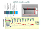
(SIMS) is an analytical technique that uses an energetic beam of ions to sputter a sample. A small fraction of the sputtered material is electrically charged, and these secondary ions can be collected and mass analysed. The strength of SIMS is not so much in quantitative analysis as for depth profiling and chemical imaging. The SIMS instrument at EMPA Thun is integrated into a dual beam SEM-FIB (Secondary Electron Microscope – Focused Ion beam) which allows excellent imaging of the sample, and very high spatial resolution SIMS measurements using the liquid metal gallium ion source primary beam (at some penalty to sensitivity compared to alternative primary ion beams). The limiting spatial resolution of the instrument is the spot-size of the primary ion beam which is about 5 nm. The use of a time-of-flight mass analyser allows all mass to charge ratios to be measured simultaneously.
The development work for this instrument was supported by the EC (part of the FIBLYS project, http://www.fiblys.eu/) with support from Tofwerk AG and Tescan a.s.
FIBSIMS
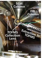
The focus of our TOFSIMS development work has been on a relative-ly low-cost versatile instrumentation module intended as an add-on to a standard high vacuum FIB chamber. Orthogonal extraction provides a high effective duty cycle and avoids the need to pulse the primary beam or to use monoisotopic gallium, thus no changes to the FIB hardware are necessary. When SIMS measurements are not required, the front part of the extraction ion optics simply clips off, thus allow-ing the full range of sample sizes to be used by the FIB. The prototype instrument has useful ion yields while depth profiling with 20 keV gallium primary ions and also chemical images with lateral resolutions of better than 40 nm are easily achieved.
J.A. Whitby et al. High Spatial Resolution Time-of-Flight Secondary Ion Mass Spectrometry for the Masses: A Novel Orthogonal ToF FIB-SIMS Instrument with In Situ AFM Adv. Mat. Sci. Engin. 2012 (1012) 180437, DOI: 10.1155/2012/180437.
In the subsequent EC-funded UnivSEM project (http://www.univsem.eu/), the sensitivity of the SIMS instrument was dramatically increased and full integration with atomic force microscopy in the electron microscope chamber achieved. This latter allows the depth in SIMS depth profiles and 3D images to be calibrated, and also allows the roughness (which affects depth resolution) to be determined accurately. The file AFM-SIMS.pptx includes video showing this.
Chemical analysis

Glow-discharge optical emission spectrometry (GD-OES) allows fast compositional depth-profiling from the nm range up to several 100 um in depths. The depth resolution of this technique is of a few nanometres for thin layers, but increases for thicker layers to reach a few percent of the total sputtered depth. The major advantages of the technique are its speed and ease of use. The spatial separation of the sputtering processes and the excitation/ionisation processes leading to the signal detection result in reliable quantification procedures, compared to surface analytical tools. A further advantage of GD-OES is its ability of qualitatively determining the hydrogen content in the sample. Though GDOES offers an excellent depth resolution it does virtually offer no lateral resolution, because the analysis area is at the best of a few mm2.

-
Share
