Novel Semiconductor Heterostructures
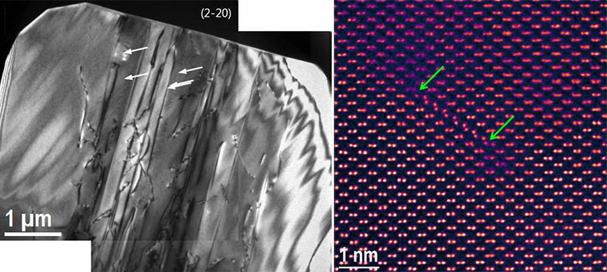
Novel technologies often require the implementation of novel materials or a new way of combining known materials. In this research topic, the electron microscopy group collaborates with other reseach groups on new semiconductor heterostructures. One sub-project concerns the development of an advanced X-ray detector based on Ge pillars grown on patterned silicon. Due to the large lattice mismatch between Si and Ge, the Ge is heavily strained due to the epitaxial growth. The strain is partially plastically relaxed by the formation of dislocations and the formation of other structural defects, like e.g. stacking faults. Characterization of these defects is crucual for advancing the understanding of their occurance as a function of growth conditions and for developping the structure-property relation of the final device.

Dislocations in a strained Ge pillar which is grown on a patterned Si substrate. High resolution image of a small stacking fault in Ge which is formed by two partial dislocations marked by green arrows. (For details see: Arroyo Rojas Dasilva et al., Appl. Phys. Lett. 107 (2015) 093501.)
This research topic is funded by the Swiss National Science Foundation and CTI, the Commission for Technology and Innovation.
-
Share
